In digital logic, a decoder is a combinational circuit that converts an n-bit binary input into exactly one active output out of a possible 2^n. A 2-to-4 decoder reads a 2-bit input and activates one of four outputs. A 3-to-8 decoder reads 3 bits and activates one of eight. Everything else in this article is detail on top of that one behaviour.
Decoders show up everywhere in digital systems: memory address selection, instruction decoding inside a CPU, driving seven-segment displays, and selecting which device on a bus gets to respond. If you have already worked through the seven-segment display article on this site, you have already seen a decoder in action without the formal name attached to it. A BCD-to-seven-segment driver is a decoder with seven outputs instead of a clean power-of-two count.
This article covers the truth table, the logic behind it, and three ways to implement a 2-to-4 decoder in Verilog, from behavioural code down to individual logic gates. Then it goes on the FPGA Learning Kit so the outputs light real LEDs instead of staying in a simulator window.
What a Decoder Actually Does
A decoder is a combinational circuit, meaning the outputs depend only on the current inputs, with no memory or clock involved. An n-input decoder produces up to 2^n outputs, and for any valid input combination, exactly one output is active while the rest sit at the opposite logic level.
Take the 2-to-4 decoder. Two inputs, A and B, select which of four outputs (Y0 through Y3) turns on:
| A | B | Y0 | Y1 | Y2 | Y3 |
|---|---|---|---|---|---|
| 0 | 0 | 1 | 0 | 0 | 0 |
| 0 | 1 | 0 | 1 | 0 | 0 |
| 1 | 0 | 0 | 0 | 1 | 0 |
| 1 | 1 | 0 | 0 | 0 | 1 |
Each row of the truth table maps directly to one output line. Y0 is active only when A=0 and B=0, which means Y0 is simply the AND of NOT-A and NOT-B. Y1 is active only when A=0 and B=1. Extend that pattern across all four outputs and you have the complete logic equations without needing a Karnaugh map, because a decoder’s truth table is already about as minimal as it gets.
Active-High vs Active-Low Outputs
Most decoder ICs you will encounter, including the classic 74HC138 (3-to-8 decoder), use active-low outputs: the selected output goes to 0 while every other output stays at 1. This is a hardware convenience, since many downstream circuits (chip selects, for example) trigger on a low signal, and NAND-based gate implementations produce active-low outputs more naturally than active-high ones. When you build the gate-level version later in this article, watch for this. The truth table above shows active-high behaviour for clarity; a 74HC138-style active-low decoder simply inverts every column.
The Enable Input
Real decoders almost always include an enable pin. When enable is off, every output is forced inactive regardless of what A and B are doing. This matters the moment you chain decoders together, for example combining two 2-to-4 decoders with enable logic to build a 3-to-8 decoder, or using enable to gate an entire address-decoding block off the bus when it is not needed. Skipping the enable input in a design that is meant to scale is a common source of bugs in early Verilog work.
What Most Beginners Get Wrong
The first is trying to write the Verilog before working out the logic on paper. A decoder is small enough that it is tempting to guess at a case statement and iterate until the simulation looks right. That approach breaks down the moment you move from a 2-to-4 decoder to a 3-to-8 or 4-to-16 decoder, where guessing is no longer fast. Write the truth table first, always, even for a circuit this small.
The second is confusing a decoder with a demultiplexer. They look almost identical in a block diagram, and the confusion is understandable, but the distinction matters once you are choosing the right block for a design. A decoder has no independent data input, it only decodes an address into a set of select lines. A demultiplexer takes a single data input and routes it to one of several outputs based on the same kind of select lines. A decoder is really a demultiplexer with its data input tied permanently high. If your circuit needs to route a signal, you want a mux or demux. If it needs to select or activate a destination, you want a decoder. We cover the demultiplexer side of this in the multiplexer and demultiplexer article.
Building a 2-to-4 Decoder in Verilog
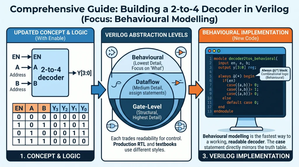
There is more than one correct way to describe the same circuit in Verilog. Each level of abstraction trades readability for control, and knowing all three matters because production RTL code and textbook examples will use different styles depending on the author and the target.
Behavioural Modelling
Behavioural modelling describes what the circuit should do, not how the gates are wired. This is the fastest way to get a working decoder and the easiest to read.
					module decoder2to4_behavioral (

    input  wire       en,

    input  wire        a,

    input  wire        b,

    output reg  [3:0]  y

);

    always @(*) begin

        if (en) begin

            case ({a, b})

                2'b00: y = 4'b0001;

                2'b01: y = 4'b0010;

                2'b10: y = 4'b0100;

                2'b11: y = 4'b1000;

                default: y = 4'b0000;

            endcase

        end else begin

            y = 4'b0000;

        end

    end

endmodule
The case statement mirrors the truth table almost line for line. This is the version to reach for when the goal is correctness and readability, and the one most synthesis tools will optimize down to the same gates as the hand-built version anyway.
Dataflow Modelling
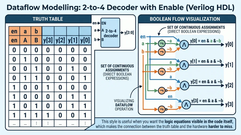
Dataflow modelling describes the circuit as a set of continuous assignments, closer to writing out the Boolean equations directly.
					module decoder2to4_dataflow (

    input  wire       en,

    input  wire        a,

    input  wire        b,

    output wire [3:0]  y

);

    assign y[0] = en & ~a & ~b;

    assign y[1] = en & ~a &  b;

    assign y[2] = en &  a & ~b;

    assign y[3] = en &  a &  b;

endmodule
Each line is the direct Boolean expression for one row of the truth table. This style is useful when you want the logic equations visible in the code itself, which makes the connection between the truth table and the hardware harder to miss.
Gate-Level Modelling
Gate-level modelling instantiates individual logic gates and wires them together by hand. This is the closest Verilog gets to drawing the schematic in text form.
					module decoder2to4_gate (

    input  wire       en,

    input  wire        a,

    input  wire        b,

    output wire [3:0]  y

);

    wire na, nb;

    not (na, a);

    not (nb, b);

    and (y[0], en, na, nb);

    and (y[1], en, na,  b);

    and (y[2], en,  a, nb);

    and (y[3], en,  a,  b);

endmodule
Two NOT gates generate the complements of A and B, then four 3-input AND gates combine enable with each input combination. This version will not appear often in real projects since synthesis tools handle gate selection far better than a human does, but building it once makes the abstraction levels above it make sense instead of feeling arbitrary.
Testbench
Every one of the three modules above needs a testbench before it goes anywhere near hardware. A short one exercises all four input combinations plus the enable line:
					module tb_decoder2to4;

    reg  en, a, b;

    wire [3:0] y;

    decoder2to4_behavioral dut (

        .en(en), .a(a), .b(b), .y(y)

    );

    initial begin

        $monitor("en=%b a=%b b=%b | y=%b", en, a, b, y);

        // enable low: every output must stay inactive

        en = 0; a = 0; b = 0; #10;

        a = 1; b = 1; #10;

        // enable high: sweep all four input combinations

        en = 1; a = 0; b = 0; #10;

        a = 0; b = 1; #10;

        a = 1; b = 0; #10;

        a = 1; b = 1; #10;

        $finish;

    end

endmodule
Swap the instantiated module name to test the dataflow or gate-level versions against the same stimulus. If all three produce identical output for every input combination, you have confirmed the abstraction levels are functionally equivalent, which is the entire point of learning all three. For a deeper walkthrough of writing and structuring testbenches, see the Verilog testbenches article.
From Simulation to Real Hardware
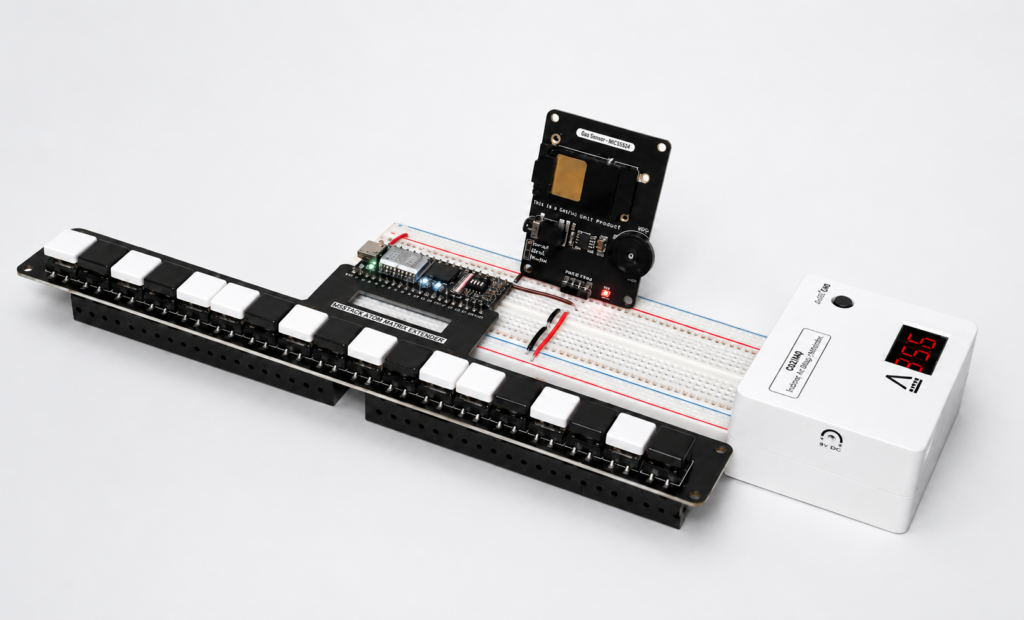
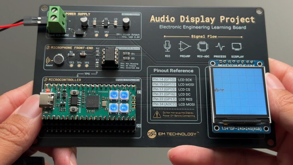
A decoder that only exists in a simulator waveform is half a lesson. The value of building this on the FPGA Learning Kit is watching four LEDs respond to physical switches in real time, with no simulator translating the behaviour for you.
Map the two inputs (A, B) and the enable line to switches or push buttons on the board, and map the four outputs (Y0 through Y3) to onboard LEDs. After synthesis and place-and-route, flipping the switches should light exactly one LED per combination, matching the truth table you started with. If two LEDs light at once, or none light at all, the fault is often in the pin constraint file rather than the Verilog itself, since a decoder’s logic is simple enough that syntax errors tend to fail at synthesis rather than produce silently wrong behaviour.
This same 2-to-4 building block scales directly. Chain two of them with shared enable logic and you have a 3-to-8 decoder: the third input bit and its inverse drive the enable pins of the two sub-decoders, so only one of the two is ever active at a time.
					module decoder3to8_structural (

    input  wire       en,

    input  wire        a,

    input  wire        b,

    input  wire        c,

    output wire [7:0]  y

);

    wire nc;

    not (nc, c);

    // c = 0 drives the low half (y0-y3), c = 1 drives the high half (y4-y7)

    decoder2to4_behavioral low_half  (.en(en & nc), .a(a), .b(b), .y(y[3:0]));

    decoder2to4_behavioral high_half (.en(en &  c), .a(a), .b(b), .y(y[7:4]));

endmodule
Two 2-to-4 decoders, one inverter, and no new logic to learn. Chain four 2-to-4 decoders the same way, gated off the outputs of a 2-to-4 decoder one level up, and you have a 4-to-16 decoder. The Verilog does not get more complicated, there is just more of it, which is exactly the kind of structural repetition FPGA design rewards once you see the pattern once.
Where Decoders Fit Next
Once a decoder is working end to end, the natural next step is either the seven-segment display driver, which is a decoder wearing a different name, or the multiplexer and demultiplexer article, which covers the inverse operation of routing a single signal out to multiple destinations. Both build on the same truth-table-first approach used here.

EIM TECHNOLOGY
Founder & Engineering Education Innovator
Daniel Cao is the Founder of EIM Technology and holds a Master of Applied Science in Engineering. With experience in engineering research, product development, PCB design, and technical education, he is the author of several books on electronics engineering. His work focuses on developing practical learning systems that integrate engineering hardware, lab instruments, curriculum, and project-based learning. Through EIM Technology, Daniel aims to make electronics and computer engineering more accessible and engaging, helping students build real experience in designing, measuring, testing, and troubleshooting electronic systems.