A multiplexer, or data selector, is a combinational circuit that selects one of several input signals and routes it to a single output, based on the value of a set of select lines. A demultiplexer, or data distributor, does the reverse: it takes one input signal and routes it to one of several outputs, again based on select lines. If a decoder activates one output based on an address, and an encoder does the opposite of a decoder, a multiplexer and demultiplexer are the data-carrying equivalent of that same idea: one selects where data comes from, the other selects where data goes.
Between the decoder article and this one, you now have the two building blocks that show up in almost every larger digital system: something that picks a destination based on an address, and something that shares one line among many signals.
This article covers how a multiplexer and demultiplexer work, builds a 4-to-1 multiplexer in Verilog across three abstraction levels, and moves it onto the FPGA Learning Kit so a real select switch drives a real output.
What a Multiplexer Does
A multiplexer, commonly abbreviated MUX, has n data inputs, a set of select lines, and one output. The number of select lines determines how many inputs can be chosen: 2 select lines address 4 inputs, 3 select lines address 8 inputs, and so on, following the same 2^n relationship you saw with decoders. Only one input reaches the output at any time, determined entirely by the current value on the select lines.
Take a 4-to-1 multiplexer. Four data inputs (D0 through D3), two select lines (S1, S0), and one output (Y). The function table below shows which data input reaches the output for each select combination, it is not a full Boolean truth table since D0 through D3 are signals rather than fixed 1s and 0s:
| S1 | S0 | Y |
|---|---|---|
| 0 | 0 | D0 |
| 0 | 1 | D1 |
| 1 | 0 | D2 |
| 1 | 1 | D3 |
Nothing about the select-line logic depends on what the data actually is. A multiplexer does not care whether D0 through D3 carry sensor readings, memory data, or clock signals, it only cares about routing whichever one is selected straight through to the output.
What a Demultiplexer Does
A demultiplexer, or DEMUX, is the mirror image: one data input, a set of select lines, and n outputs. The select lines determine which single output receives the input data, while every other output is driven to logic 0.
A 1-to-4 demultiplexer with select lines S1 and S0 sends the single input D to one of four outputs (Y0 through Y3):
| S1 | S0 | Active Output |
|---|---|---|
| 0 | 0 | Y0 = D |
| 0 | 1 | Y1 = D |
| 1 | 0 | Y2 = D |
| 1 | 1 | Y3 = D |
If this looks familiar, it should. A demultiplexer with its data input tied permanently high is structurally identical to a decoder: the select lines become the decoder’s address inputs, and the single active output line becomes the decoder’s active output. This is why a decoder is often described as a demultiplexer without a real data input, a point covered in more depth in the decoder article.
What Most Beginners Get Wrong

The confusion that costs the most time is not between multiplexers and demultiplexers themselves, which are at least clearly opposite operations. It is confusing the select lines with the data.
Beginners writing their first multiplexer testbench frequently vary the data inputs and forget to sweep the select lines through all their combinations, or the reverse: they hold the data steady and only vary the select lines without ever confirming the mux actually forwards different data values correctly. An exhaustive sweep of every input combination catches both problems at once, but for a beginner still learning what a mux does, splitting the test into two targeted sweeps, one isolating the select path and one isolating the data path, makes it far easier to tell which part of the circuit is wrong when something fails.
The second common mistake is trying to build a demultiplexer as if it were a completely different circuit from a decoder or multiplexer, instead of recognizing it is the same select-line logic with the data path added. Once you can write a decoder, a demultiplexer is a small extension, and once you can write a multiplexer, understanding a demultiplexer as its structural opposite becomes far easier than learning it from scratch.
Building a 4-to-1 Multiplexer in Verilog
As with decoders, there is more than one way to describe the same multiplexer in Verilog, and each style makes a different part of the logic explicit.
Behavioral Modeling
					module mux4to1_behavioral (

    input  wire [3:0] d,

    input  wire [1:0] sel,

    output reg         y

);

    always @(*) begin

        case (sel)

            2'b00: y = d[0];

            2'b01: y = d[1];

            2'b10: y = d[2];

            2'b11: y = d[3];

            default: y = 1'b0;

        endcase

    end

endmodule
The case statement reads almost exactly like the function table: whatever sel holds selects the matching bit of d. This is the version to reach for first, since it is the easiest to verify against the function table by eye.
Dataflow Modeling
					module mux4to1_dataflow (

    input  wire [3:0] d,

    input  wire [1:0] sel,

    output wire        y

);

    assign y = (~sel[1] & ~sel[0] & d[0]) |

               (~sel[1] &  sel[0] & d[1]) |

               ( sel[1] & ~sel[0] & d[2]) |

               ( sel[1] &  sel[0] & d[3]);

endmodule
This is the sum-of-products form: each term is active for exactly one select combination, and only that term’s data bit passes through to the output. It is more verbose than the behavioral version but makes the underlying Boolean logic visible instead of hidden inside a case statement.
Gate-Level Modeling
					module mux4to1_gate (

    input  wire [3:0] d,

    input  wire [1:0] sel,

    output wire        y

);

    wire ns1, ns0;

    wire t0, t1, t2, t3;

    not (ns1, sel[1]);

    not (ns0, sel[0]);

    and (t0, d[0], ns1, ns0);

    and (t1, d[1], ns1, sel[0]);

    and (t2, d[2], sel[1], ns0);

    and (t3, d[3], sel[1], sel[0]);

    or  (y, t0, t1, t2, t3);

endmodule
Four AND gates each gate one data input against its matching select condition, and a single OR gate combines the results. Since only one AND gate can be active for any given select value, the OR gate effectively just passes through whichever term is live.
Testbench
					module tb_mux4to1;

    reg  [3:0] d;

    reg  [1:0] sel;

    wire        y;

    mux4to1_behavioral dut (

        .d(d), .sel(sel), .y(y)

    );

    initial begin

        $monitor("d=%b sel=%b | y=%b", d, sel, y);

        // fixed data pattern, sweep every select combination

        d = 4'b1010;

        sel = 2'b00; #10;  // expect y = 0 (d[0])

        sel = 2'b01; #10;  // expect y = 1 (d[1])

        sel = 2'b10; #10;  // expect y = 0 (d[2])

        sel = 2'b11; #10;  // expect y = 1 (d[3])

        // fixed select, change the data to confirm it passes through

        sel = 2'b10;

        d = 4'b0100; #10;  // expect y = 1 (d[2])

        d = 4'b1011; #10;  // expect y = 0 (d[2])

        $finish;

    end

endmodule
This testbench deliberately runs two separate sweeps, one holding the data steady while the select lines change, and one holding the select steady while the data changes, which is the exact distinction called out earlier in this article. Passing both sweeps is what actually proves the multiplexer works, not just one of them. For more on structuring a testbench like this, see the Verilog testbenches article.
Building the Demultiplexer
A 1-to-4 demultiplexer reuses the same select-line decoding, with the data input gating each output instead of an enable signal:
					module demux1to4_dataflow (

    input  wire       d,

    input  wire [1:0] sel,

    output wire [3:0] y

);

    assign y[0] = d & ~sel[1] & ~sel[0];

    assign y[1] = d & ~sel[1] &  sel[0];

    assign y[2] = d &  sel[1] & ~sel[0];

    assign y[3] = d &  sel[1] &  sel[0];

endmodule
Compare this to the decoder’s dataflow module from the decoder article: the structure is identical except en has been replaced with d. That is not a coincidence, it is the same circuit with the enable line repurposed to carry actual data.
From Simulation to Real Hardware
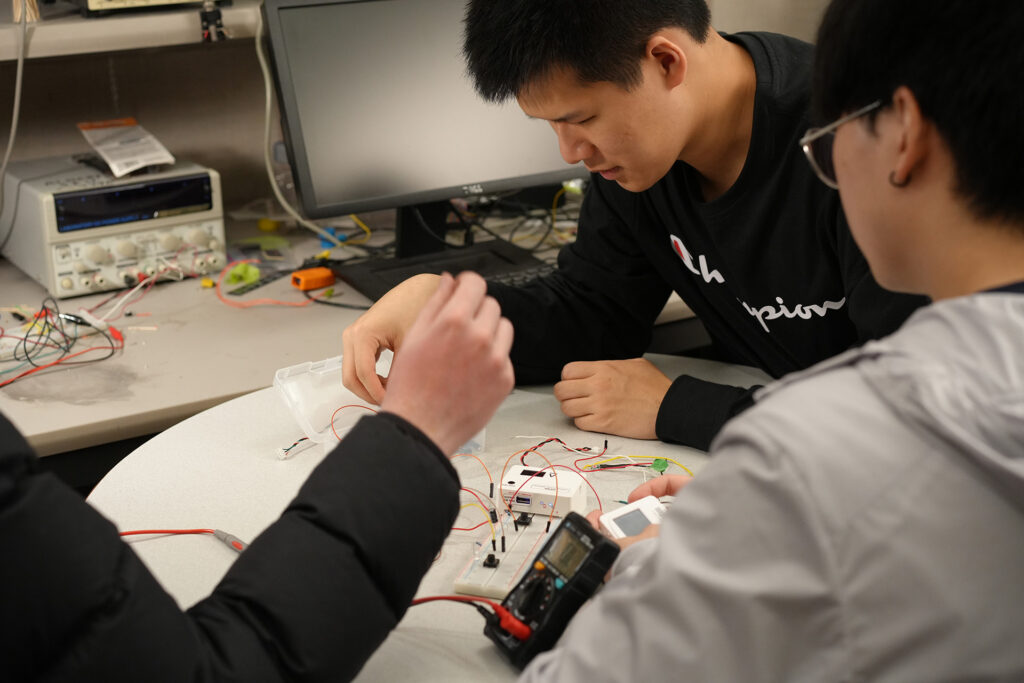
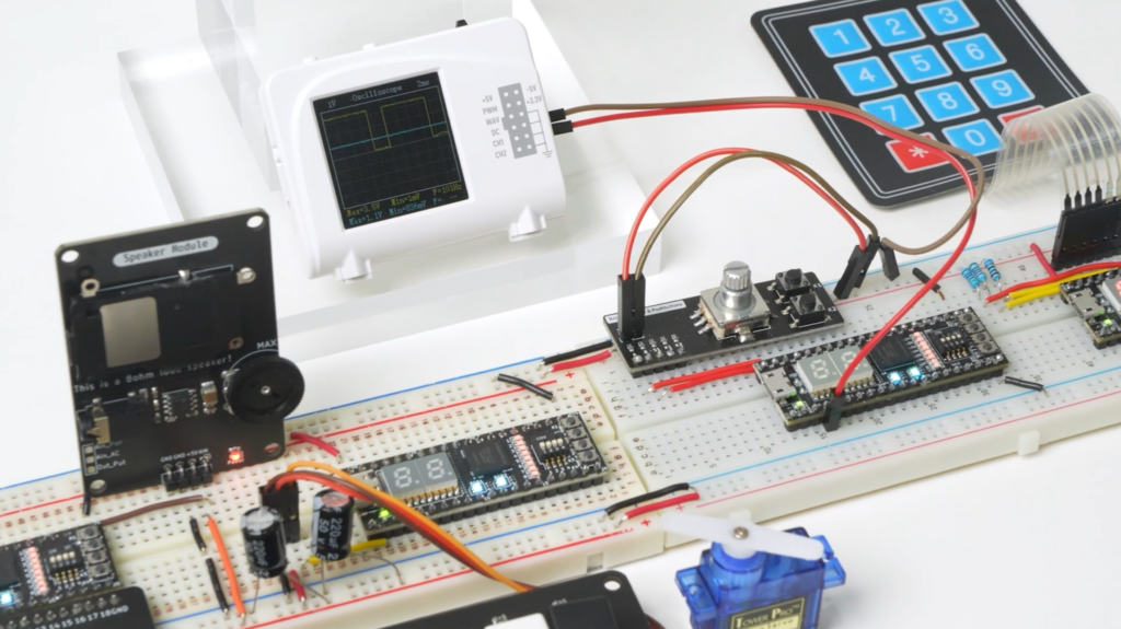
On the FPGA Learning Kit, map the two select lines to two switches, the four data inputs to four more switches (or hardcode a fixed pattern directly in the top-level Verilog module to save pins), and the single output to an LED. Flipping the select switches should move the LED’s state to match whichever data input is currently selected, live, with no simulator between you and the hardware.
The demultiplexer is the more visually convincing of the two builds on real hardware: wire the single data input to one switch and the four outputs to four LEDs, then flip the select lines and watch the active LED jump from one position to another while the other three stay dark. It makes the select-line logic obvious in a way that reading a function table does not.
This same 4-to-1 structure scales the same way decoders do. Two 4-to-1 multiplexers plus one more select line and a final 2-to-1 stage build an 8-to-1 multiplexer: the top select bit picks which of the two 4-to-1 outputs reaches the final output.
					module mux8to1_structural (

    input  wire [7:0] d,

    input  wire [2:0] sel,

    output wire        y

);

    wire y_low, y_high;

    mux4to1_behavioral low_half  (.d(d[3:0]), .sel(sel[1:0]), .y(y_low));

    mux4to1_behavioral high_half (.d(d[7:4]), .sel(sel[1:0]), .y(y_high));

    assign y = sel[2] ? y_high : y_low;

endmodule
Two 4-to-1 multiplexers evaluate in parallel, and the top select bit, sel[2], picks between their outputs with a single 2-to-1 selection. This is the identical divide-and-combine pattern used to build a 3-to-8 decoder out of two 2-to-4 decoders.
Where This Fits Next
With a decoder, a multiplexer, and a demultiplexer built, you have the core set of data-selection blocks used throughout digital design. The natural next step is either the shift register article, which introduces sequential logic and a clock into the picture for the first time, or back to the seven-segment display driver, which is a decoder problem wearing a display’s wiring.

EIM TECHNOLOGY
Founder & Engineering Education Innovator
Daniel Cao is the Founder of EIM Technology and holds a Master of Applied Science in Engineering. With experience in engineering research, product development, PCB design, and technical education, he is the author of several books on electronics engineering. His work focuses on developing practical learning systems that integrate engineering hardware, lab instruments, curriculum, and project-based learning. Through EIM Technology, Daniel aims to make electronics and computer engineering more accessible and engaging, helping students build real experience in designing, measuring, testing, and troubleshooting electronic systems.