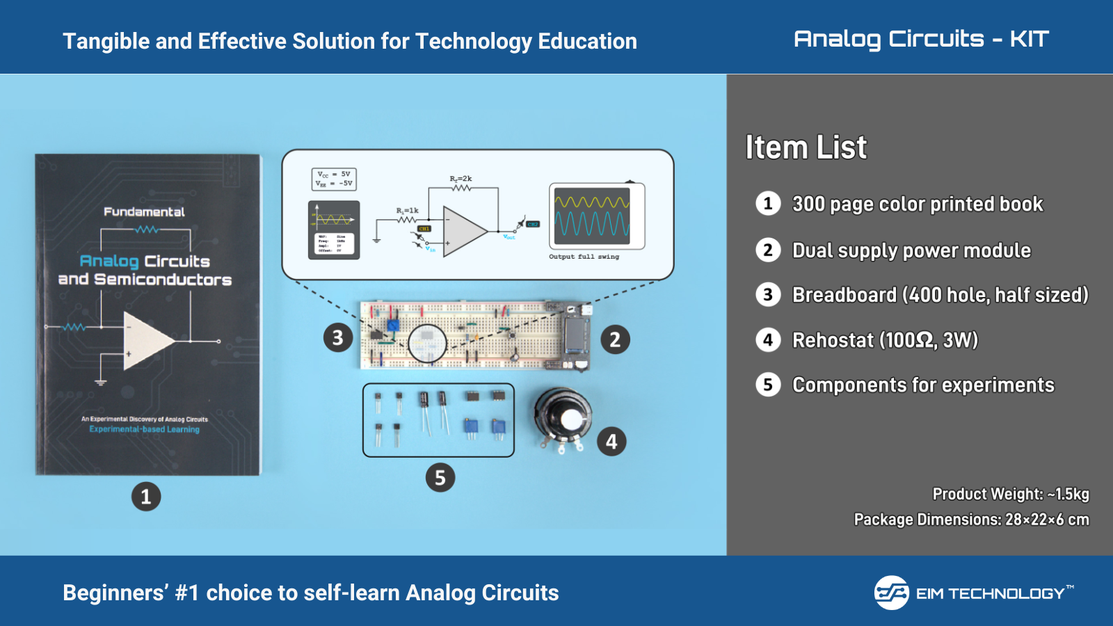
A flip-flop is an electronic device, specifically a type of memory component, capable of storing one bit of data. It has two states, "SET" and "RESET," which are represented by the binary values 1 and 0, respectively. The flip-flop maintains its current state until it receives a signal prompting it to switch to the opposite state. A clock or pulse signal can "trigger" the flip-flop to change state.
What is a D flip flop?
A D flip-flop, also known as a D-type or data flip-flop, is a digital storage element utilized in sequential logic circuits. It captures the value of the D (data) input at a specific part of the clock cycle, typically on the rising or falling edge of the clock signal, and holds this value until the next clock event. Hence, they are also known as Delay Flip Flop. Here is an overview of its main features and functionality:
Components and Symbols
- Inputs:
- D (Data): The input value to be stored.
- Clock (CLK): The control signal that determines when the D input is sampled.
- Reset (optional): A control signal that can reset the output to a predefined state (usually 0).
- Set (optional): A control signal that can set the output to a predefined state (usually 1).
- Outputs:
- Q: The stored value.
- Q': The complement of the stored value (optional).
D FLIP FLOP Symbol
The typical symbol for a D flip-flop in circuit diagrams looks like a box with the following labels:

D flip flop waveform

When the clock signal is low, the flip flop holds its current state and ignores the D input.
When the clock signal is high, the flip flop samples and stores D input.
The value that was previously fed into the D input is reflected at the flip flop’s Q output.
If D = 0 then Q will be 0.
If D = 1 then Q will be 1.
The Q’ output of the flip flop is complemented by the Q output.
If Q = 0 then Q’ will be 1.
If Q = 1 then Q’ will be 0.
Functionality:
- Data Capture: On the rising (or falling) edge of the clock signal, the value at the D input is sampled and transferred to the Q output.
- Data Hold: The value at the Q output remains constant until the next clock edge, regardless of changes in the D input during the interim period.
- Reset/Set (if present): The reset or set inputs can override the clock control to force the output to 0 or 1, respectively.
D flip flop truth table
Here’s a truth table summarizing the operation of a D flip-flop without reset and set inputs:

Characteristic Table of D Flip Flop
The characteristic table of the D flip flop displays the behavior of the flip flop for each combination of input and current state. The characteristic table for a D flip flop is as follows.

Characteristics table of D Flip Flop
- D is the input, and Q is current state, Qn + 1 is the next state outputs.
- Qn+1 will always be zero when D is 0, irrespective of current state of flip flop.
- When the input of the flip flop is 1, next state of flip flop will always be 1, regardless of the current state of flip flop.
Characteristic Equation of D Flip Flop
The characteristics equation of D flip flop consist of a Boolean expression that explains the relationship between the input and output of the flip flop. The characteristic equation for a D flip flop is as follows.
Qn+1 = D
Characteristics Equation of D Flip Flop
- Qn+1 represents the output of flip flop at the next clock cycle.
- D is the input to the flip flop at the current clock cycle, and n represents the current clock cycle.
- This characteristic equation of D flip flop states “that the output of the flip flop at the next clock cycle will be equal to the input at the current clock cycle“.
D Flip Flop Excitation Table
An excitation table is derived from the truth table.

Qn represents the current state of the flip flop, and D represents the current input of the flip flop. Where as Qn+1 represents the next state of the flipflop.
- When the Qn is 0 and the D is also 0, then the Qn+1 becomes 0. This situation explains the condition of “hold” state.
- When the Qn is 0 but D is 1, then the Qn+1 becomes 1. This situation explains the condition of “reset” state.
- When the Qn is 1 but D is 0, then the Qn+1 becomes 0. This situation explains the condition of “hold” state.
- When the Qn is 1 and the D is also 1, then the Qn+1 becomes 1. This situation explains the condition of “reset” state.
Ripple Through: a significant limitation of a D flip flop

The figure above demonstrates a potential issue with level-triggered D-type flip-flops: if the data input changes while the clock pulse is at its high level, the logic state at Q will change in response to D, ultimately retaining only the last input state during the clock pulse (period RT in above figure). This phenomenon is known as ‘Ripple Through.’ Although this characteristic allows the level-triggered D-type flip-flop to function as a data switch, passing data from D to Q while the clock signal (CK) is at logic 1, it may not be desirable in many circuit applications.
Types of D Flip Flop
- D Latch.
- Edge Triggered D Flip Flop.
Applications of D Flip Flop:
D flip-flops are fundamental building blocks in digital electronics and are used for:
- Data Storage: Storing individual bits of data.
- Shift Registers: Constructing shift registers that can shift data serially or in parallel.
- Counters: Forming the basis of binary counters.
- Synchronization: Synchronizing asynchronous signals to a clocked domain.
- State Machines: Implementing the state memory in finite state machines (FSMs).
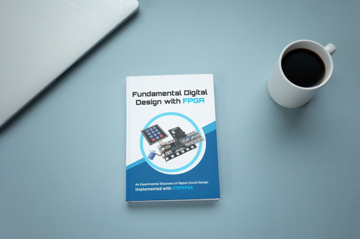
See the practical working of D flip flop using FPGA Board:
EIM Technology’s FPGA board for beginners allowing you to efficiently study the working and implementations of the sequential logic circuits.
D-flip flop Verilog code:
module tb_d_flip_flop;
// Testbench signals
reg D;
reg CLK;
reg RESET;
wire Q;
// Instantiate the D flip-flop
d_flip_flop uut (
.D(D),
.CLK(CLK),
.RESET(RESET),
.Q(Q)
);
// Clock generation
always #5 CLK = ~CLK;
initial begin
// Initialize signals
CLK = 0;
D = 0;
RESET = 0;
// Apply reset
#10 RESET = 1;
#10 RESET = 0;
// Apply test vectors
#10 D = 1;
#10 D = 0;
#10 D = 1;
#10 D = 1;
#10 D = 0;
// Finish simulation
#50 $finish;
end
// Monitor signals
initial begin
$monitor("Time = %0t, D = %b, CLK = %b, RESET = %b, Q = %b", $time, D, CLK, RESET, Q);
end
endmodule
Easily run this code on FPGA board and observe the desired out.
https://www.eimtechnology.com/collections/all-products/products/step-fpga-development-board
GET 15% OFF ON FPGA BOARD & FPGA KIT >> https://www.eimtechnology.com/collections/all-products/products/digital-electronics-with-fpga-learning-kit-with-fpga-tutorials

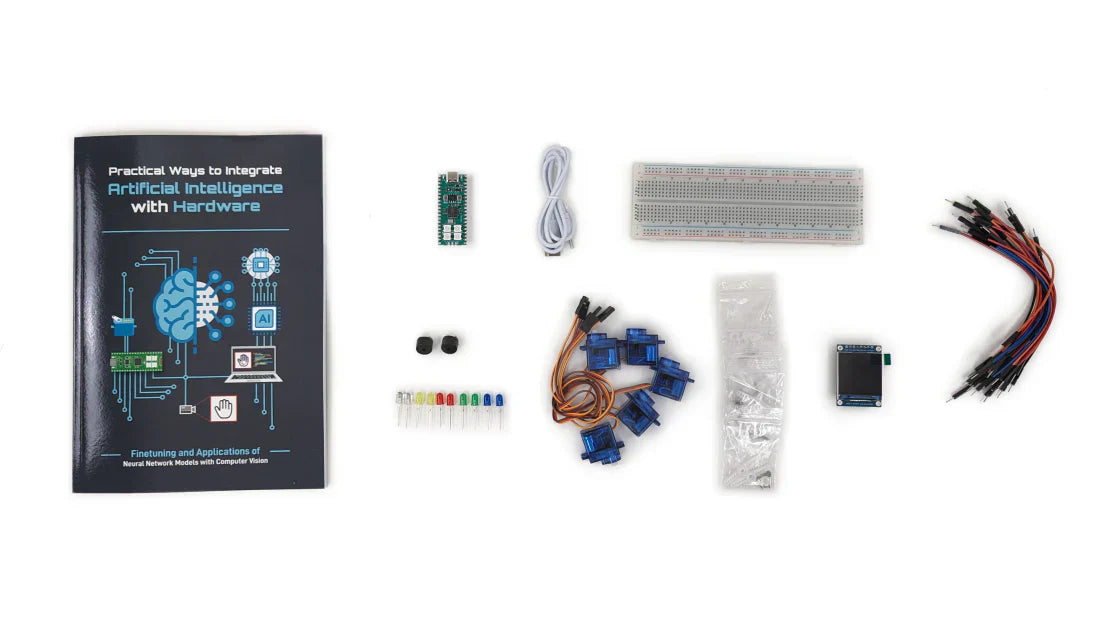
Check our FPGA learning kit / Digital Circuits DIY kit

D flip-flops are crucial components in synchronous digital circuits, providing reliable storage and state control synchronized with a clock signal. They are extensively used in various digital systems, including memory elements, data registers, and control circuits.